Highest Resolution Electrical Measurements

Posted on November 15, 2016 by Amster
Palo Alto, California – November 15, 2016 PrimeNano Inc. announces the release of the new and improved version of ScanWave™ – ScanWave™ 1.5. Like its predecessor, is a stand-alone module for most benchtop atomic force microscopes (AFMs). It enables nanoscale imaging and measurements of the permittivity and conductivity of materials, but now with even more impressive capabilities. Recent advances include quantitative doping characterization of semiconductor devices1.
ScanWave™ 1.5 comes with a 20-30% improvement in system sensitivity and SNR. It features a redesigned probe interface, improved probes and upgraded software. ScanWave™ 1.5 incorporates advanced technologies resulting in almost double the sensitivity of dC/dV Amplitude and Phase measurements2. As a result of the improvements in ScanWave™ 1.5, it is significantly easier to use and gives the user better electrical property imaging in less time and with less effort.
Improved Probes:
A better impedance match of the probe and probe loader increases sensitivity of measurements.
A new and more user friendly probe and probe loader design makes loading and unloading easier and faster.
An improved reflectometer (RF) software update allows prompt verification of a working electrical contact.
Upgraded Software:
Improved system stability.
Improved user interface makes it easier to setup for measurements.
Advanced Technology:
Improved sMIM electronics and technology: increases resolution, sensitivity, and contrast all at the same time.
Doubled the range of channel signal adjustment means easier AFM alignment before measurement, which results in time savings.
Here is an example to show you the improvement:
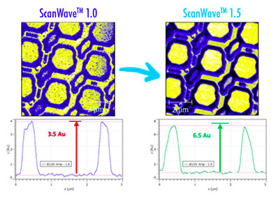
CMOS image sensor measured with 500mV applied AC bias (0V DC)
ScanWave™ 1.5 maintains all key features of ScanWave 1.0:
* Allows 6 Channels of Data in One Single Scan.
* Supports Subsurface Imaging.
* Allows Simultaneous Imaging of Different Classes of Materials.
* Has Minimal Sample Prep Time.
* Does Not Require Conductive Path.
* Supports Contact and Non-Contact Mode Imaging.
Upgrade option is available from Scanwave™ 1.0.
PrimeNano, with the latest sMIM technology, is continuing to work with academia and industry to push the envelope for next generation materials for microelectronics, energy, data storage and applied physics.
1 ScanWave measures the relative variation of the permittivity and conductivity if the probe-sample interface. Using a calibrated doped reference sample, ScanWave can make quantitative measurements of doped semiconductor devices.
2 PrimeNano demonstrated 30nm resolution features in the sMIM-C channel and 20nm for the dC/dV Amplitude image using a SRAM NFET test sample, front side polish 32nm logic device. Contact us for details of test.
Copyright 2024. All Rights Reserved