Highest Resolution Electrical Measurements

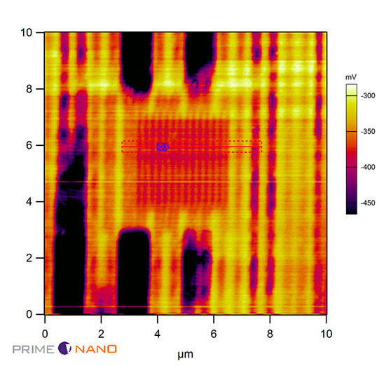
Buried Grating under 100nm Si from a Back-side Polished Logic Device
Image of sMIM-C channel showing a buried grating structure under 100nm of silicon wafer left after backside polishing the die of logic devices. The grating structure has a fine pitch of 250nm spacing. The sMIM-C image shows defects and other details that confirm a resolution less than 100nm, even though the image was acquired through the 100nm thickness of the Si over-layer.
Copyright 2024. All Rights Reserved