Highest Resolution Electrical Measurements

Buried SiO2 Structures Under Si3N4 Film
PrimeNano fabricated a test sample to illustrate sensitivity to local permittivity even when buried beneath the sample surface. The sample contains patterned SiO2 structures under a Si3N4 film. The nitride surface was polished to eliminate any residual topographic features. Figure 1 (a) shows a cross-sectional schematic of the test sample. A blanket SiO2 film was deposited, patterned and eteched to produce 90 nm thick features with lateral dimensions on the order of 5 μm. A thick nitride film was then deposited and polished flat. After processing the nitride film is 280 nm thick, leaving 190 nm of nitride on top of the 90 nm thick oxide features. The oxide and nitride film thicknesses were confirmed by optical interferometry.
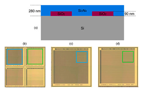
Figure 1 (a) The PrimeNano buried structure reference sample was fabricated on a Si wafer. 90 nm thermal SiO2 was grown on the wafer and patterned. 1um LPCVD Si3N4 was deposited to fully cover the SiO2. CMP was usedto polish the sample until the Si3N4 is about 280 nm; (b) Photo of the 4 quadrant reference sample. Each quadrant has a different patterned structure; (c) blue highlighted quadrant is a 10μm pitch positive square structure 5μm x 5μm; (d) green highlighted quadrant is a 10μm pitch 5μm wide line structure. All the structures are 90nm thick SiO2.
The sample die contains 4 patterns in 4 quadrants as shown in Figure 1 (b). (c) Shows the upper left quadrant with a pattern of 5μm x 5μm squares on a 10μm pitch (highlighted in blue); and (d) shows the upper right quadrant with 5 μm wide lines on a 10μm pitch.
Because the oxide and nitride are both insulating, there is no variation in conductivity over the sample so the MIM signal will only have a capacitive response from the permittivity difference between the SiO2 features (e = 3.9)and the Nitride film (e = 7.5). This is illustrated in Figure 2.
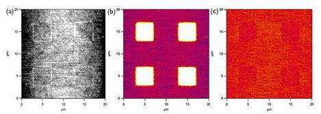
Figure 2 (a) Topography image of polished Si3N4 film on buried SiO2 patterned structure; (b) sMIM-C channel image showing higher capacitance (brighter) contrast over buried SiO2 structures under 200nm Si3N4 film; and (c) the sMIM-R channel image which shows no conductive signal.
Figure 2 shows (a) the topography of the polished reference surface with a roughness less than 1nm in the imaged area; Figure 2 (b) and (c) show the sMIM-C and sMIM-R channels respectively. As expected there is no signal in the sMIM-R channel. In the sMIM-C channel we see bright regions where the buried square structures are sensed under the nitride layer. The ScanWave™ senses the difference in permittivity of the 90nm thick SiO2 feature under the nitride film compared to where there is only the 280nm Nitride film. Where there is a SiO2 feature the sMIM measures a lower capacitance than where there is no feature and represents this as a “brighter” region. The greater the relative difference in dielectric value of the buried material to the cap layer the larger the sMIM contrast and the deeper the buried feature can be sensed.
Copyright 2024. All Rights Reserved