Highest Resolution Electrical Measurements

Determining the Resolution of SMIM Using Donor Structures

Dr. David Scrymgeour received his PhD in Material Science from Penn State and is currently a staff scientist at Sandia National Laboratories. His research interests include using scanning force techniques for the characterization of quantum material systems as well as ferroelectric, metallic, and complex oxide surfaces.
In the following Applied Surface Science paper lead/co-lead by Dr David Scrymgeour and Dr. Shashank Misra, the lateral resolution limits of sMIM are probed by examining nanostructures in silicon created through phosphorous doping using hydrogen resist lithography. This paper opens up the application of sMIM to studying quantum material systems.
Determining the resolution of scanning microwave impedance microscopy using atomic-precision buried donor structures
By David Scrymgeour et al. Applied Surface Science, 2017
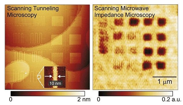
The creation of atomically precise dopant structures of phosphorous within silicon using scanning tunneling microscope (STM) based hydrogen resist lithography is an ideal platform for testing the fabrication limits of doping in silicon. This technique creates highly conductive two dimensional sheets of ultra-dense phosphorus dopant nanostructures 10s to 100s of nanometers below the silicon surface with theoretical precision down to the placement of single phosphorous dopants. This technology has been pushing the limits of fabrication and has been used by many groups to create nanowires, dots, and single dopants, and could prove to be a core building block of silicon based quantum computing devices.
The nondestructive investigation of these buried phosphorus nanostructures presents several unique challenges, the two biggest being locating the buried nanostructures for creation of electrical contact to them and providing metrology on donor layer quality and layout. We show in this work that sMIM is an ideal tool for probing these silicon nanostructures and, by turning the problem on its head, we can create atomically precise calibration structures that we use to study the resolution of the sMIM technique itself. We found that we can resolve line spacing down to ~80 nm, and surprisingly, that tip wear does not change the resolving power of the tip significantly, indicating a complex relationship between tip apex, material properties, and resolving power that warrants more study.
To read the original publication of this paper, please visit Applied Surface Science.
A selected list of Dr. Scrymgeour’s relevant publications:
1. D. A. Scrymgeour et al, "Determining the resolution of scanning microwave impedance microscopy using atomic-precision buried donor structures,” Applied Surface Science, 423, pages 1097-1011, (2017).
2. JF Ihlefeld et al, “Domain imaging in ferroelectric thin films via channeling-contrast backscattered electron microscopy,” Journal of Materials Science, 52, 2, pages 1071-1081 (2017).
3. JF Ihlefeld et al, “Room-Temperature Voltage Tunable Phonon Thermal Conductivity via Reconfigurable Interfaces in Ferroelectric Thin Films,” Nano Letters, 15, 3, 1791-1795 (2015).
Contact the author: Dr. David Scrymgeour.
Copyright 2024. All Rights Reserved