Highest Resolution Electrical Measurements

Enclosed Objects And Processes In Liquids
Dr. Alexander Tselev received his PhD in Materials Sciences from Dresden University of Technology, Germany. He spent terms at University of Maryland, College Park, Georgetown University, Duke University, and the Center for Nanophase Materials Sciences at ORNL in University of Tennessee, Knoxville. Currently his primary research focus is on near-field microwave microscopy and complex oxide thin films. He has published more than 150 papers in refereed journals.
In this freshly released ACS Nano paper co-led by Dr. Alexander Tselev from ORNL’s Center for Nanophase Materials Sciences and Dr. Andrei Kolmakov from NIST’s Center for Nano Science and Technology, a new paradigm for in situ in-liquid imaging at the micro- and nano-scale is introduced. The implementation harnesses the longer range sensitivity of near-field microwaves. An excerpt of the paper is reproduced here:
Seeing through Walls at the Nanoscale: Microwave Microscopy of Enclosed Objects and Processes in Liquids
By Alexander Tselev & et al. ACS Nano, 2016.
In situ imaging at the nanoscale in liquids and gases provides a wealth of insights into biomedical and electrochemical systems and processes, helping to understand, gain control, and to optimize them. Such imaging can, in principle, be achieved with use of high-energy electrons or X-rays, with specimens being enclosed into environmental cells filled with liquids or gases. However, in many cases of interest, the high-energy particles and radiations are destructive, triggering unwanted sample chemical transformations. The radiolysis can be so intense that any reasonable imaging turns out to be impossible. Furthermore, high-energy particles and radiation are fundamentally denied for studies of delicate, low-energy processes and collective excitations. In turn, microwaves photons of a few gigahertz frequencies and energies ~10 μeV affect neither electronic states, nor chemical bonds in condensed matter.
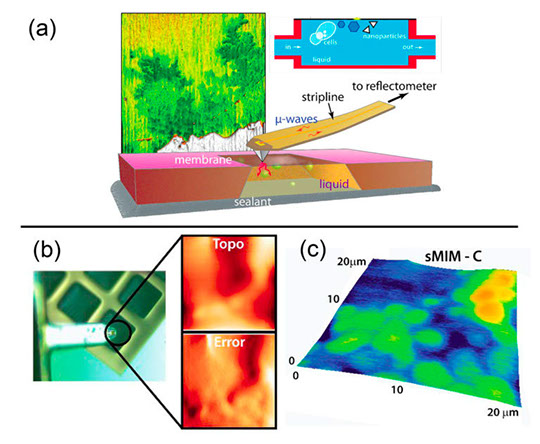
(a) Layout of the experimental setup for near-field scanning microwave impedance microscopy in liquids. An AFM-type scanning probe is integrated into an AFM setup for probe scanning over the sample surface with control of the probe-sample distance and force. The objects under study are enclosed in a capsule filled with a fluid (or gas) and separated from the probe by an ultrathin dielectric membrane transparent for microwave radiation. The capacitance and conductance of the tip−sample system are monitored by a microwave reflectometer operating at a frequency of 3 GHz. Left inset: 40 μm x 40 μm in situ microwave near-field image of Ag dendrites electrochemically grown at a Ag electrode in a 102 mol/m3 AgNO3 water solution. The image was obtained through a 50 nm SiN membrane. (b) A photo of the probe with a set of 8 nm thick SiO2 membranes underneath, with cavities filled with a liquid and live yeast cells. The images near the photo are topographic and deflection error images over an 8 nm membrane. (c) Near-field microwave image of the yeast cells under the 8 nm.
A scanning microwave impedance microscope was used to demonstrate the non-destructive, high-resolution imaging of electrochemical processes and live biological cells in liquids. In contrast to traditional in situ use of scanning probes, when probes are immersed in a liquid, in the new technique, probes are separated from the liquid and specimen’s environment by ultrathin molecular-impermeable, dielectric membranes with samples being encapsulated into environmental cells. This approach results in full isolation of a specimen and its environment from ambient as well as the rest of the microscope, additionally providing a great flexibility for application of other analytical techniques. Microwave near fields formed at the sharp scanning probe penetrate through the dielectric membranes and liquid, which allows sensing and mapping nanoscale objects and their dielectric properties. The thinnest, 8 nm-thick, SiO2 membrane used in the work showed an excellent mechanical stability in contact with the scanning probe. It is of importance that since encapsulation of specimens into environmental cells is used for in situ electron and X-ray microscopy, much effort was dedicated in recent years to development and microfabrication of closed or fluidic environmental cells equipped with ultrathin membranes. This creates a solid base for a rapid development of the technique.
Through a side-by-side comparison of the microwave imaging with scanning electron microscopy, advantages of microwaves for artefact-free, non-invasive, imaging are revealed in the paper. The spatial resolution of microwave imaging obtained with the commercially available system exceeds the resolution of optical microscopy for similar samples and is comparable to that of in situ liquid-cell scanning electron microscopy. It is clear that the membrane thickness can be further reduced to increase spatial resolution and sensitivity of the imaging.
To read the original publication of this paper, please visit ACS Nano.
Dr. Alexander Tselev’s Research
The groundbreaking research and recent publications of Dr. Tselev demonstrates the exciting new categories of research were Scanning Microwave Impedance Microscopy (sMIM) opens new ground to the research community, both for advanced materials research and commercial applications. PrimeNano applauses Dr. Tselev’s novel application of sMIM technology and look forward to where his creativity will lead the field in the future.
A sample list of Dr. Tselev’s recent publications:
- A Tselev & et al. “Microwave a.c. conductivity of domain walls in ferroelectric thin films”. Nature Communications 7 (2016); http://dx.doi.org/10.1038/ncomms11630.
- T Monti & et al. “High-resolution dielectric characterization of minerals: a step towards understanding the basic interactions between microwaves and rocks”. International Journal of Mineral Processing 151, 8–21 (2016); http://dx.doi.org/10.1016/j.minpro.2016.04.003.
- A Tselev & et al. “Surface control of epitaxial manganite films via oxygen pressure”. ACS Nano 9 (4), 4316-4327 (2015); http://dx.doi.org/10.1021/acsnano.5b00743.
- A Tselev & et al. “Quantitative nanometer-scale mapping of dielectric tunability”. Advanced Materials Interfaces 2, 1500088 (2015); http://dx.doi.org/10.1002/admi.201500088.
- L Collins & et al. “Probing charge screening dynamics and electrochemical processes at the solid-liquid interface with electrochemical force microscopy”. Nature Communications 5 (2014); http://dx.doi.org/10.1038/ncomms4871.
- A Tselev & et al. “Scanning Near-field microwave microscopy of VO2 and chemical vapor deposition graphene”. Advanced Functional Materials 23 (20), 2635-2645 (2013); http://dx.doi.org/10.1002/adfm.201203435.
Contact the author: Dr. Alexander Tselev.
Copyright 2024. All Rights Reserved