Highest Resolution Electrical Measurements

Measuring Quantum Hall Effect and HeTe Quantum Wells using LT ScanWave™
LT ScanWaveTM is the latest PrimeNano innovation available to market. LT ScanWaveTM enables electrical characterization of materials at ultra-low temperatures and high magnetic field. LT ScanWaveTM's technology has already put to use in research like the study of quantum Hall effect in graphene stripes at 5 K and 9 T, and HgTe quantum Wells at 9 T. Here are summaries of these two research.
Graphene Stripes – Quantum Hall Effect
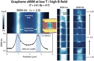 One compelling example from the Shen Lab is the direct imaging of a conductivity transition in single layer graphene triggered by the filling of bulk landau levels in the quantum Hall effect regime (figure 1). The grounded single layer graphene stripe is sandwiched between two 20 nm layers of boron nitride and sits on a 300 nm oxide on a doped Si wafer. As the bias on the Si wafer is changed, carriers are driven in or out of the graphene, changing the occupancy of Landau states. When a Landau level becomes fully occupied, the bulk graphene becomes insulating. This is shown for the = 2.0 Landau level filling in figure 1 where the dark regions are low conductivity. The bright regions at higher and lower partial fillings of Landau levels (eg. = 2.35 or 1.75) and at the edges are conductive regions. Furthermore, this conductivity change is being observed through a 20 nm thick insulating BN layer and is an excellent example of sMIM’s ability to directly observe fundamental electrical properties even through insulating over-layers. It is important to note that measuring these phenomena could only occur through performing sMIM measurements in a cryogenic environment with a strong magnetic field, showing that the LT-sMIM System is a uniquely capable tool.
Figure 1 High resistance at integer filling of Landau levels in a Graphene stripe, along with persistent conductivity from edge states. Courtesy of Y. Cui, Stanford University.
HgTe Quantum Wells – Unexpected Edge Conduction
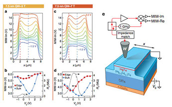 In 2015 the Shen lab showed compelling sMIM results [1], which involved sMIM measurements in a He4 cryostat with a 9 Tesla superconducting magnet [2] on an HgTe quantum well (QW), which is a topological insulator; device shown schematically in Fig. (2e). Measurements were performed on two QW devices – HgTe/ (Hg0.3Cd0.7)Te of thicknesses 5.5 and 7.5 nm, which correspond to thicknesses above and below the threshold of 6.7 nm predicted by Quantum spin Hall (QSH) theory, above which, edge conduction is expected. Experiments were performed at 4.5K and the expected QSH behavior was confirmed at zero magnetic field – only the 7.5 nm device displayed edge conduction, while the 5.5 nm device did not (results not shown here, see [1]).
However, when time reversal symmetry is broken by introducing the magnetic field, it was shown that the edge conduction in the 7.5 nm device survived up to 9 T with no signs of diminishing, which was well beyond the expected crossover field of 3.8 T – an unexpected result. The sMIM results at 4.5 K and varying magnetic field (0-9 Tesla) combined with transport measurements provided an opportunity to learn the physics beyond the textbook QSH theory, a rare occurrence in the field of topological insulators, where up until the Shen lab results, theoretical predictions were routinely confirmed. This highlights the enormous potential of the LT-sMIM System to elucidate the nature of the fundamental mechanisms at the cutting edge of our understanding.
Figure 2 Transport and MIM line-cut analysis for the 7.5nm device at 3 and 7 T. (a) Averaged line-cuts of the real-space MIM-Im acquired at 3 T with a 1.0V offset in MIM signal between each gate voltage. Gate voltage is from -1.5 to 3.0V in steps of 0.5V. (b) Edge and bulk MIM-Im signal (at the red and blue dashed lines in a) and two-terminal resistance plotted against gate voltage. (c,d) Same plots for the 7 T real-space MIM-Im images. Transport is clearly dominated by edge conduction in the bulk gapped regime in both fields, confirming the extended nature of the edge conduction observed by MIM. Panel (e) shows a schematic of MIM set-up and device structure, showing line scan direction x. [1]
References
- E.Y. Ma, M.R. Calvo, J. Wang, B. Lian, M.Muhlbauer, C. Brune, Y.T. Cui, K. Lai, W. Kundhikanjana, YL Yang, M. Baenninger, M. Konig, C. Ames, H. Buhmann, P. Leubner, L.W. Molenkamp, S.C. Zhang, D. Goldhaber-Gordon, M.A. Kelly, Z.X. Shen. Unexpected edge conduction in mercury telluride quantum wells under broken time-reversal symmetry. Nature Communications, 6, 7252 (2015).
- Kundhikanjana, W., Lai, K., Kelly, M. A. & Shen, Z.-X. Cryogenic microwave imaging of metal-insulator transition in doped silicon. Rev. Sci. Instrum. 82, 033705 (2011).
To read more about how you can conduct your research in similar setup, visit LT ScanWaveTM product page.
Copyright 2024. All Rights Reserved