Highest Resolution Electrical Measurements

SCANWAVE PRO™ - New product with the industry’s best performance
PERFORMANCE
- Breakthrough sensitivity of < 0.10 aF
-
Unmatched Signal to Noise
- Improvement of >10x over other systems
- Nanoscale spatial resolution
-
High power for subsurface imaging
- Depth range >200 nm
- Proprietary shielded probes
- Streamlined probe exchange
BENEFITS
- Measure variations in permittivity and conductivity ( ε & σ ) at the nanoscale
- Multiple AFM modes supported such as Contanct, Non-Contact, Tapping, PeakForce Tapping, Datacube & Lift Mode
-
Characterize a variety of electrical properties with these channels:
- sMIM-C, sMIM-R, sMIM dC/dV, dR/dV, and C-V
- Little to no sample preparation required
- Electrical measurements on insulating substrates
- Subsurface imaging for buried structures
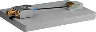
- Tool-less probe exchange
- Asylum and Bruker AFMs supported (specific models)
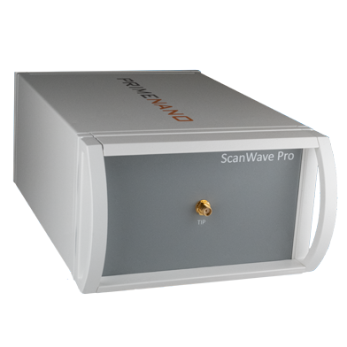
ScanWave ProTM
Tool less Probe Holder
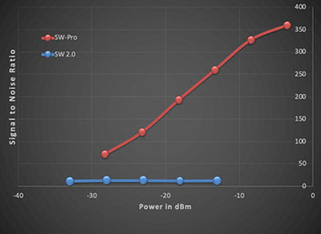
Signal to Noise comparison for ScanWave ProTM vs ScanWave 2.0TM
APPLICATION EXAMPLES
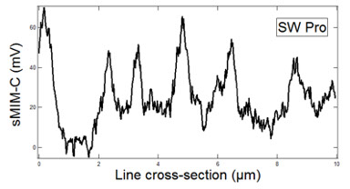
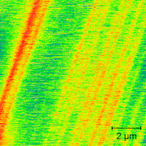
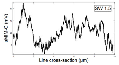
1. sMIM AC Mode Imaging of Carbon Nano Tubes (CNT) on Sapphire
ScanWave Pro™ has a much higher signal to noise ratio than ScanWave 1.5™. The plots to the right of the images are single line profiles extracted from the corresponding images to the left.
ScanWave Pro™ increases the usefulness of sMIM in AC/Tapping Mode enabling imaging of fragile samples with reduced tip wear even in low signal applications.
ScanWave ProTM
ScanWave 1.5TM
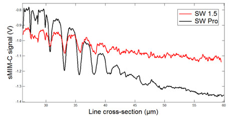
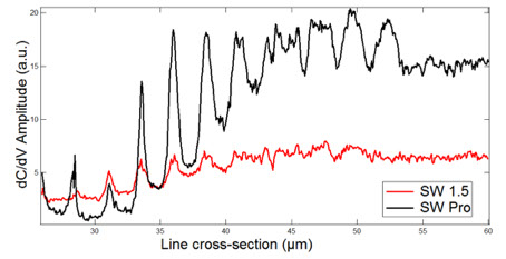
2. Enhanced Sensitivity to Dopant Concentration
Below are comparison plots of single line cross sections of sMIM-C (top) and sMIM dC/dV amplitude (bottom) taken across a doped staircase reference sample. The staircase is p-doped with a step-by-step decreasing dopant concentration from left to right. The dopant level sensitivity of ScanWave Pro™ is more than 2 orders of magnitude better than ScanWave 1.5™.
3. Highest Quality Subsurface Imaging
Offering the highest subsurface imaging capability in the industry, the ScanWave Pro™ enables high resolution imaging of buried features.
Shown below is an sMIM image of a repeating SiO2 structure buried beneath 190nm of Si3N4. There is no topographical information on this sample because its surface was polished. However, sMIM can clearly image the buried structures due to the permittivity difference between the oxide and nitride surrounding it.
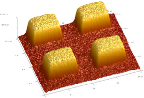
ScanWave ProTM image of buried structures
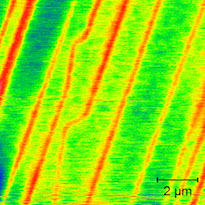
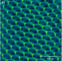
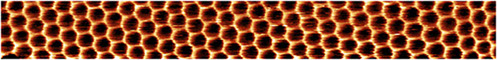
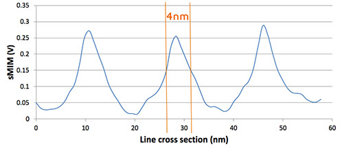
4. Moiré Pattern of Graphene on Hexagonal Boron Nitride
When two different regular patterns are superimposed, the pattern that emerges has a different periodicity and it is called a moiré pattern. Shown below is the moiré pattern crated by the superposition of a single layer of graphene on a thin layer of boron nitride (h-BN) imaged using ScanWave Pro™. The periodicity of the moiré pattern depends on the twist angle between the graphene and the h-BN.
While there is no contrast in the topography, the contrast in the ScanWave signal shows the honeycomb pattern with a period of 14 nm (Figures a & b). A line cross section (Figure c) indicates a sharp transition in the honeycomb pattern with ~4 nm lateral spatial resolution (FWHM).
(b)
(c)
Interested to Know More?
To learn more about the ScanWave Pro™, or if you want to upgrade from a ScanWave 1.5, please contact us by clicking the Contact PrimeNano button below.
Copyright 2024. All Rights Reserved