Highest Resolution Electrical Measurements

Spontaneous Domain Walls In Ferroelectric Crystals
Ferroelectric materials possessing spontaneous polarizations have been widely employed in data storage1,2 and nano-scale transistor devices3. In these applications ferroelectric domains are purposefully polarized for device structures to realize certain functions. In recent years, the ferroelectric domain walls (DWs), where the order parameter changes drastically within a narrow width (sub-to-few nanometers) 4-8, have become the subject of intense scientific research9-11. In particular, the unexpected electrical conduction at ferroelectric DWs12-15 is highly attractive because of the possibility to create and control nano-scale 1D/2D conductive paths in wide band gap insulators.
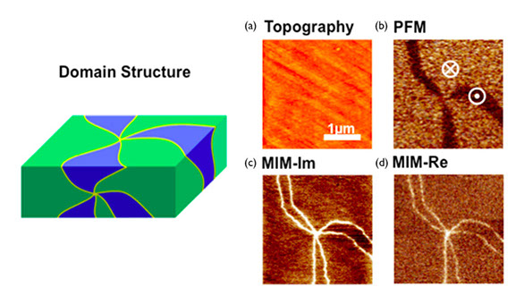
Figure 1 Domain walls on a 001 plane surface of ErMnO3 ferroelectric crystal. The schematic represents the domain walls along the different planes illustrating the expected cross-sectional view. (a) the topography shows a smooth polished surface, (b) is a nano-mechanical pulsed force image of the domain. The contrast shows the domain regions. Images (c) sMIM-C and (d) sMIIM-R show the domain walls are conductive instead of the expected insulating. The images also suggest surface charging is present.
Previous studies on the ferroelectric domain structures often relied on chemically etching the ferroelectric or on piezoresponse force microscopy, both of which can damage the device. These methods provide limited information and also may induce unexpected responses under tip bias. DW conductivity studies have been predominantly carried out using C-AFM. This is not an ideal technique to study the local conductivity in bulk ferroelectrics. When using C-AFM, a DC voltage is applied between the conductive tip and a counter electrode on the sample. The measured current flow depends highly on the actual current path in the sample as well as the tip-sample Schottky barrier9,15. Relatively large voltages (up to 10 V) are typically needed in order to tunnel through the barrier. These conditions result in unwanted nonlinear responses and contribute to complicated interpretations of c-AFM results.
Scanning microwave impedance microscopy (sMIM) is an ideal technique for the study of ferroelectric materials. The measurement technique is non-destructive, requires minimal sample preparation, and measures local permittivity and conductivity properties of samples at the nano-scale without requiring a conductive path. Furthermore, the surface topography and domain configuration can be simultaneously acquired.
Here we show a typical scanning result on LiTaO3 sample. The sample was prepared by polarizing a commercially available z-cut LiTaO3 crystal with congruent composition and single domain. As shown in the domain structure schematic, up and down domains were created with polarization perpendicular to the sample surface, i.e., the c+ and c– directions. Figure 2 (a), a topographic image of the sample, verifies there are no features present and the surface is flat. Figure 2 (c) and (d) are the Amplitude and Phase of the piezoelectric response to a tip sample bias (i.e. PFM image) .The contrast in the phase image clearly shows the opposite polarizations of the two domains. Interestingly, in Figure (e) and (d) the sMIM images, sMIM –C and sMIM –R respectively, indicate that the DWs are more conductive than the domains. Based on the finite element method (FEM) simulation, the DW conductivity is estimated to be about 1000 S/m.
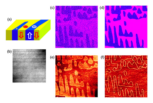
Figure 2 (a) schematic of an induced polarization of a LiTaO3 material with up-down domain orientation as shown with the white and red arrows. Imagase (b) the topography, (c) Piezo Force response (PFM) amplitude and (d) PFM phase differentiate the domain directions; images (e) sMIM-C and (d) sMIM-R also provide the domain information but in addition are more sinsitive and also DW condictivity information.
Unlike C-AFM that measures the current flow through the full sample depth along a varied path, sMIM measures only the desired local conductivity near the tip apex (or at sample surface). Based on the researcher’s experimental data and theoretical study, the tested DWs are only conductive at the surface with the conductivity due to surface charge effects. A 1D conductive DW is induced by the surface lattice reconstruction caused by the surface charge. A 1D conductive channel is very rare in general. The sample studied here is stabilized in the unlikely environment of a big gap insulator by lattice rigidity perpendicular to ferroic distortion. This mechanism opens a door to make novel nano-scale structures by fabricating conductive 1D/2D paths on an insulating matrix.
Use of ScanWave™ benefits researchers with better understanding of the physics and reveals important insights on these novel mechanisms. Better understanding of the ferroelectric domain structures will result in novel engineering designs for ferroelectric-based devices.
References:
- Waser, R. & Rüdiger, A. Pushing towards the digital storage limit. Nat. Mater. 3, 81–82 (2004).
- Cho, Y., Hashimoto, S., Odagawa, N., Tanaka, K. & Hiranaga, Y. Nanodomain manipulation for ultrahigh density ferroelectric data storage. Nanotechnology 17, S137–141 (2006).
- Scott, J. F. Applications of modern ferroelectrics. Science 315, 954–959 (2007).
- Yamanouchi, M., Chiba, D., Matsukura, F. & Ohno, H. Current-induced domain-wall switching in a ferromagnetic semiconductor structure. Nature 428, 539–542 (2004).
- Ravelosona, D. et al. Domain wall creation in nanostructures driven by a spin-polarized current. Phys. Rev. Lett. 96, 186604 (2006).
- Yang, T., Gopalan, V., Swart, P. & Mohideen, U. Direct observation of pinning and bowing of a single ferroelectric domain wall. Phys. Rev. Lett. 82, 4106–4109 (1999).
- Meier, D. et al. Anisotropic conductance at improper ferroelectric domain walls. Nat Mater 11, 284–288 (2012).
- Jia, C.-L. et al. Atomic-scale study of electric dipoles near charged and uncharged domain walls in ferroelectric films. Nat Mater 7, 57–61 (2008).
- Schröder, M. et al. Conducting domain walls in lithium niobate single crystals. Adv. Funct. Mater. 22, 3936–3944 (2012).
- Hanson, J. N., Rodriguez, B. J., Nemanich, R. J. & Gruverman, a. Fabrication of metallic nanowires on a ferroelectric template via photochemical reaction. Nanotechnology 17, 4946–4949 (2006).
- Haussmann, A., Milde, P., Erler, C. & Eng, L. M. Ferroelectric lithography: bottom-up assembly and electrical performance of a single metallic nanowire. Nano Lett. 9, 763–768 (2009).
- Guyonnet, J., Gaponenko, I., Gariglio, S. & Paruch, P. Conduction at domain walls in insulating Pb(Zr0.2 Ti0.8)O3 thin films. Adv. Mater. 23, 5377–82 (2011).
- Seidel, J. et al. Conduction at domain walls in oxide multiferroics. Nat Mater 8, 229–234 (2009).
- Farokhipoor, S. & Noheda, B. Conduction through 71° domain walls in BiFeO3 thin films. Phys. Rev. Lett. 107, 3–6 (2011).
- Choi, T. et al. Insulating interlocked ferroelectric and structural antiphase domain walls in multiferroic YMnO3. Nat Mater 9, 253–258 (2010).
Copyright 2024. All Rights Reserved