Highest Resolution Electrical Measurements

Buried Stored Charge In SRAM Flash Memory
Flash memory is present on an ever-increasing variety of integrated circuits. Many design validation, reverse engineering and national security tasks benefit significantly from direct imaging of the data bit patterns that are created by the presence and absence of stored charge on the floating gates of the flash memory cells. No technology exists today to directly measure the stored charge. sMIM has shown itself to be sensitive to the extremely small change in the electric field induced in the Si layer above the stored charge, enabling detection of the stored charge in a single FLASH memory cell.
A commercial FPGA chip was first programmed with a repeating pattern. The device was then de-processed and polished from the backside so that the residual silicon thickness was from 100’s of nm’s to 0nm. The shallow bevel was used to determine the optimal Si thickness for the sMIM signal strength. It was determined that between 90-120nm was optimal. Below are images acquired using the ScanWave™ integrated with an Oxford Instruments Asylum Research MFP-3D AFM. An area of approximately 500mm was imaged and stitched together manually to validate the methodology for large area applications.
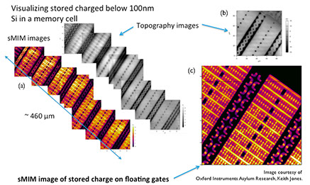
Figure 1 shows (a) 8 images of topography and sMIM stitched together, (b) a single topography image 90μm region, and (c) a single sMIM image 90 area with clearly visible bright regions identifying the stored charge FLASH cells.
Figure 1. (a) shows a stitched array of 8, 90 x 90 μm images. The top image is the topography and the bottom the MIM image optimized to provide the best contrast of the stored charge locations in the images. The images were collected using contact mode scanning. The two enlarged singles images, (b) and (c) are the topography and sMIM respectively. In the enlarged sMIM image the individual stored charge are clearly visible as brighter dots. The topography image showed no detail related to the stored charge or individual cells.
Figure 2 shows another example reading stored charge from a back-side polished FLASH memory array. In this example the data was collected in a non-contact imaging mode. The device was programmed with a repeated pattern and prepared similarly as described above. An Oxford Instruments Asylum Research Cypher AFM was used to image the stored charge FLASH RAM array using the PrimeNano shielded probes. The images in Figure 2 (a) the sMIM-C and (b) sMIM-R were acquired by mechanically actuating the cantilevers at their resonance frequency and using a second lock-in to collect the sMIM data at the same frequency as the cantilever resonance. Using the 2nd lock-in to collect the sMIM data results in dC/dZ measurement where sMIM-C & -R data channels are collected at the signal maximum providing a high level of Signal-to-Noise (SNR) in the sMIM image. The two images show very clearly the stored charge bits (brighter bits) in the cell locations. The data is circled for clarity.
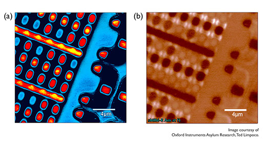
Figure 2. ScanWave™ module integrated with an Asylum Research Cypher AFM sMIM measurement of stored charge on a backside polished FLASH array using non-contact imaging. Image (a) is the sMIM-C signal using a Lock-in amplifier to the same frequency as the cantilever resonance; (b) is the sMIM-R signal using the same Lock-in arrangement. Both images can be acquired at the same time.
sMIM measurements on these stored charge samples have been repeated multiple times. In each case the data acquired with the ScanWave™ was straight forward and required no special setup. The sample preparation is crucial to the consistent quality of the electrical sMIM measurement. The feasibility of imaging over an entire memory array, stitching the data together, and then reading the “1’s” and “0’s” is now a realistic capability.
Copyright 2024. All Rights Reserved