Highest Resolution Electrical Measurements

Characterization Of Insulated-Gate Bipolar Transistor
Vertical Insulated Gate Bipolar Transistors (IGBTs) are one of the most important types of discrete power transistors. These devices were developed to have more efficient operation and faster switching. The IGBT combines the simple gate-drive characteristics of MOSFETs with the high-current and low-saturation-voltage capability of bipolar transistors.1
In general, for power transistors, the two key parameters are blocking voltage, namely the maximum voltage the device can block in the off-state, and the on-state resistance, which should be as low as possible. Both IGBTs and MOSFETS are commonly fabricated with trench gates. The trench gates allow increases in both the blocking voltage and the on-state operating current.2
Investigation of device performance involves many different types of mechanical and electrical testing. Understanding the doping level and carrier type at different locations in the device is critical to the design and performance of IGBT devices. Cross-section and front facing polish are two common methods for preparing a sample to expose the active device layers for standard dopant profile measurements. sMIM can be applied to these same samples to gain a more nuanced view of the device structure beyond just the doping and carrier type information.
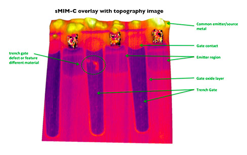
Figure 1. MIM capacitive data overlaid with the topography demonstrating the dynamic range of the mode to image metals, doped regions, and insulators in a single image. The image shows greater detail than other electrical modes on doped cross-sectioned samples
Figure 1 is the sMIM-C (capacitive) overlaid to the topography of an IGBT device prepared for PrimeNano by ChipWorks. The dynamic range of a sMIM measurement includes metals, doped regions, and dielectric materials and the image clearly shows features such as the dielectric gate oxide layer, the metallic gate contact, and the semiconducting emitter region as well as defects that are likely residue from the polishing process. The detail in the image demonstrates the range of the MIM technique.
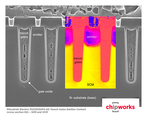
Figure 2. SEM image with SCM insert of a cross-section preferentially etched IGBT device. SCM image saturates in gate trench and metals. Emitter and doped substrate are represented with little detail.
An SEM and corresponding SCM image measured by Chipworks on a similar IGBT device, Figure 2, shows a cross-section through the emitter, the cross section shows the emitter connecting directly to the tungsten contact strip. The tungsten contacts appear to have been back-etched, rather than subjected to chemical mechanical polish (CMP).2
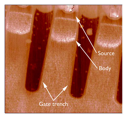
Figure 3 sMIM dC/dV Amplitude image of cross-section IGBT. The image highlights the source and body doped regions with high level of detail. The gate trench region with details of polish residue.
A similar IGBT part was prepared for PrimeNano for imaging with the ScanWave™ System. The sMIM technique provides a level of information that usually requires both the SEM and SCM to provide the full level of device structural detail. It is possible to consider using sMIM may remove the requirement to preferentially etch doped samples for SEM imaging, a time consuming and highly skilled process, thus shortening the workflow. sMIM also provides additional information over SCM having better sensitivity and higher resolution.
ScanWave™ has as a standard functionality the ability to image the sample and provide 6 additional channels of data, dependent on the specific AFM capabilities. The standard MIM-C &R channels are related to the sample’s permittivity and conductivity. With the application of a modulated bias to the sample either through the ScanWave™ probe or the sample holder we can collect the dC/dV and dR/dV Amplitude and Phase for an additional 4 images; information similar to SCM but with more sensitivity and easier to get a signal response than traditional SCM.
For most semiconductor applications the dC/dV amplitude and phase provide important information about the carrier concentration and carrier polarity respectively. Figure 3 show the IGBT Amplitude of a couple of gate trench features with a level of detail not seen in the SCM image shown previously. The source and body, as well as the metal plug can be clearly identified. The n-p-n transitions from the source-to-body-substrate do not exhibit fuzzy boundary transitions typical of the SCM images.
The use of sMIM in characterizing IGBT, and semiconductor devices in general, benefit from the increased sensitivity to the material, insensitivity to linear materials (metals, insulators, and dielectrics) traditionally requiring secondary techniques to image. The ScanWave™ uses shielded probes and optimized electronics to achieve an ease of use that improves the workflow of device characterization.
References
- Wikipedia, IGBT, Entry; http://en.wikipedia.org/wiki/Insulated-gate_bipolar_transistor
- Chipworks Website, URL; http://www.chipworks.com/en/technical-competitive-analysis/resources/blog/competitive-analysis-igbts-reveals-internal-workings/
Copyright 2024. All Rights Reserved