Highest Resolution Electrical Measurements

Low Dopant Level Measurements in Semiconductors Using ScanWaveTM
ScanWave™ is an sMIM (scanning Microwave Impedance Microscopy) implementation that has been through several revolutionary improvements to achieve unprecedented sensitivity in measuring capacitance, dopant levels in semiconductors and resistivity in a variety of materials. In this technique, an AFM cantilever is used as a microwave source to measure the electrical properties of materials with nanometer lateral resolution. An sMIM measurement provides the local permittivity and conductivity of films. From this measurement we derive dopant concentration and dopant polarity in semiconductors. For example, in semiconductor manufacturing, dopant levels range from intrinsic (pure silicon) up to degeneratively doped levels that reach into a few tens of percent of the silicon lattice (1E21 a/ cm3 doping = ~20% of silicon atoms). The sMIM signal will respond to any concentration of dopant but the resolution of the measurement and absolute sensitivity must be such that extremes on either end of the dopant range used in manufacturing of semiconductor devices can be imaged. That range is from approximately 1E12 a/cm3 to 1E22 a/cm3.
While several electrical AFM techniques can be used to characterize dopant concentration between E15 a/cm3 to E20 a/cm3, it becomes difficult to measure dopant concentration at the lower end of the spectrum. As sMIM measures inherent capacitance of a sample, it is not limited by the dopant concentration. Previously, it was shown that ScanWave™ can resolve the dopant concentration between E15 to E20 a/cm3. In this article, we show the sensitivity of the ScanWave™ system for low doped concentrations varying from intrinsic silicon to E15 a/cm3. Overall, this gives the ability to measure about 10 decades of variation in the dopant concentration “without breaking a sweat”.
In this study, we prepared samples with varying amounts of dopant concentration at the low end of the doping spectrum. Phosphorus was the species used which is an n-type dopant in silicon. In Figure 1, we show the response of sMIM-C (local capacitance of the semiconductor) in Volts for these samples. There is clear differentiation of the sMIM-C signal between the dopant levels. Theoretically, sMIM can detect dopant level variations from intrinsic silicon all the way to degenerative levels but this is the first time that low doped silicon was measured well below E15 a/cm3 levels.
Even though dynamic SIMS has the highest sensitivity of any analytical technique, there are species/matrix interaction limitations that reduce this sensitivity substantially. For phosphorus in silicon the sensitivity of SIMS is impacted by mass interference between P and SiH that is formed during sputtering. An additional advantage of sMIM is that there are no limitations due to species and matrix interactions so any type of dopant can be imaged at the same level of sensitivity. Also notable is that the response of sMIM to dopant concentration is linear and can be accurately modeled so that the entire range of useful levels can be easily quantitatively imaged.
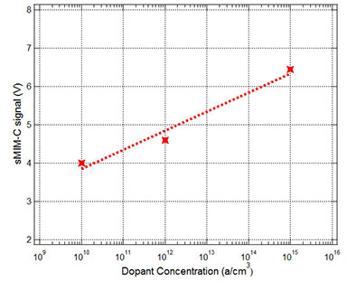
Figure 1 sMIM response with varying dopant concentration
Download
this Paper
Copyright 2024. All Rights Reserved