Highest Resolution Electrical Measurements

SCANWAVE PRO™ SOLUTIONS - Automated Quantified Dopant Measurements
KEY FEATURES
-
Automated Quantification of Dopants
- Accurate, calibrated dopant images
-
Nanoscale Dopant Spatial Resolution
- 10 nm lateral resolution
-
Widest Detection Range of Dopant Levels
- Intrinsic silicon to 1E20 a/cm3
-
Identifies Dopant Polarity
- N or P Type Identified
-
Stable and Repeatable
- Repeatability better than 0.1 of a decade of dopant level
BENEFITS
- Fast & Automated Quantification
- Highest sensitivity to dopants in the industry
-
Better insight into your measurements
- Quantified results solve problems
- Little to no sample preparation required
- Electrical measurements on insulators
- Tool-less probe exchange
- Bruker Dimension Icon AFM supported
PRODUCT DESCRIPTION
-
Software
- AFM Measurement Automation
- Calibration Process Automation
- Image Processing and Presentation
-
Hardware
- Enclosure temperature control unit to 0.1°C/hr
- Reference sample and holder
- 100 – 240 V AC
- 500 W Max
- Requires ScanWave Pro™
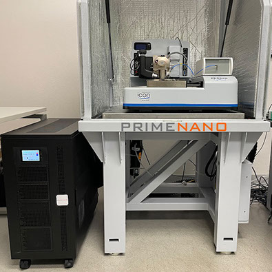
ScanWave ProTM Solutions Hardware
ScanWave Response to Dopant Concentration
from Intrinsic Silicon to 1E19 a/cm3
APPLICATION EXAMPLES
1. Quantified Image of Doped Epitaxial Silicon
The unprecedented lateral resolution combined with the industry’s highest sensitivity provide detailed dopant maps and depth profiles. Show in Figure 1 is the dopant concentration map and depth profile of two face-to-face assembled epitaxially grown and doped silicon samples. The false color map represents dopant levels with nanoscale positional precision. The dopant type (n or p) is determined, and color coded in the map below. Operations on the false color map such as line cross sections (also shown below), point readout and more are standard in this system. This map is automatically generated by the ScanWave ProTM Solutions system.
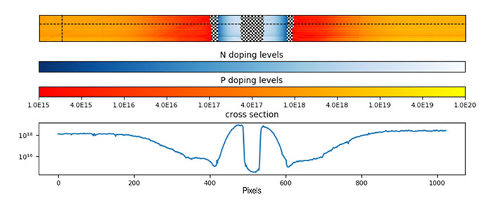
Figure 1 Dopant Concentration Map in atoms/cm3 and Corresponding Depth Profile
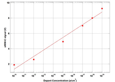
2. Industry’s Highest Sensitivity to Dopant Levels
ScanWave ProTM Solutions achieves sensitivity to low dopant levels never before possible without very expensive, complicated and destructive techniques such as SIMS. The log-linear response of ScanWave to dopant concentration (Figure 2) facilitates accurate and repeatable quantification of results for any level of dopant used in chip production today.
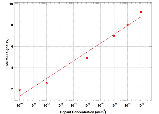
Figure 2 ScanWave Response to Dopant Concentration from intrinsic Silicon to 1E19 a/cm3
3. High Repeatability Measurements
Dynamic repeatability was measured using a reference standard and found to be better than 1/10 of a decade of concentration (Figure 3) for each of the dopant levels in the sample (1E15 to 1E20 a/cm3). The ScanWave ProTM Solutions temperature control unit achieves stable temperature in the enclosure of 0.1 °C/hr guaranteeing ultimate repeatability. Failure analysis and process monitoring using ScanWave ProTM Solutions is now fast, repeatable, and easy to perform.
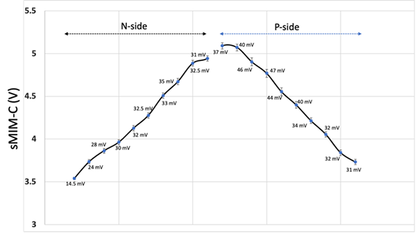
Figure 3 Capacitance Signal (Volts) Repeatability for Staircase Sample
Interested to Know More?
Download Brochure
Contact PrimeNano
To learn more about the ScanWave ProTM Solutions, please contact us by clicking the Contact PrimeNano button below.
Copyright 2024. All Rights Reserved