Highest Resolution Electrical Measurements

SMIM Sheds New Light On What’s Inside Technology

Benedict Drevniok joined Chipworks, a TechInsights company, 2 years ago. He is currently pursuing his PhD in Physics at Queens University in Kingston, Canada. His research revolves around the behavior of technologically relevant molecules on metallic surfaces, and metallic surfaces coated with ultra-thin insulating layers. Additionally, this work involves the design and operation of a scanning tunneling microscope. Benedict’s background in Scanning Probe Microscopy has prepared him for the challenges of semiconductor industry technology and patent verification. He is the resident expert for sMIM and is the primary user of the technology adoption at Chipworks.
 St. J Warren-Dixon (Sinjin) has been in the field of semiconductor and failure analysis for more than 20 years. He has a PhD in Chemical Physics from University of Toronto. Since 2006, Sinjin has been managing the Chipworks Process Analysis Engineering team, while his previous positions focused on semiconductor reverse engineering analysis with hands on experience with Scanning Probe Microscopy, SEM, with a particular focus on characterizing doped semiconductors. Sinjin brings a unique perspective and expertise that has kept Chipworks as an industry leader for technology patent validation, and verification.
For over 20 years Chipworks, a TechInsights company, has been a trusted patent and technology partner to the world’s largest and most successful companies. Business leaders rely on Chipworks to help them identify and fully leverage their most valuable patents and provide crucial analysis of high-revenue products in the most competitive, fastest changing technology markets.
In this recently published article at Chipworks.com, how sMIM is allowing a better look into the electrical characteristics of latest technologies is examined. Specifically, the imaging of the pixels of the OmniVision OV2D7AG, a CMOS image sensor, is discussed.
sMIM Sheds New Light on What’s Inside Technology
Contributed by: B. Drevniok – Chipworks, O. Amster – Prime Nano Inc. and St. J. Dixon-Warren – Chipworks
Scanning microwave impedance microscopy (sMIM) is a new scanning probe microscopy (SPM) technique that replaces traditional scanning capacitance microscopy (SCM). Like SCM, the new sMIM technique reveals information on the implanted dopant structures of a semiconductor device. The sMIM technology provides the traditional dC/dV SCM images, which give insight into the dopant types and the positions of junction, while also providing several other channels of information, including sMIM-C and sMIM-R. The sMIM-C signal is proportional to the permittivity/capacitance variation, which, for semiconducting samples, depends on the carrier concentration, since highly doped materials will give lower capacitance for the tip-sample contact than low doped materials. The sMIM-R channel provides information about the conductivity of the sample.
Chipworks recently partnered with PrimeNano Inc. of Palo Alto California, the leading supplier of sMIM technology. As a result of this partnership, Chipworks has added the PrimeNano ScanWave™ sMIM technology to our Bruker SPM and has jointly presented a paper at the recent ISTFA 2015 Conference, in Portland, Oregon. The results presented in this paper are summarized below.
The PrimeNano ScanWave™ sMIM technology sends a 3 GHz microwave signal down a specially shielded SPM probe, shown schematically in Figure 1. The resulting near-field electromagnetic wave at the probe tip interacts with the sample surface and a portion of the microwave power is reflected back along the shielded path to the detection electronics. The higher sensitivity of the sMIM electronics combined with the shielded probes, allows the direct measurement of the capacitance information, sMIM-C, as compared to conventional SCM, which requires a lock-in technique to extract the capacitive response of doped samples. The additional information provided by sMIM brings a number of benefits. The image contrast is more robust and the technique is less sensitive to artifacts induced by sample preparation, resulting in faster data acquisitions times and higher quality images. sMIM can also measure linear (metals and dielectrics) and non-linear (doped semiconductors) simultaneously. This gives information about variations in dielectric materials as well as metallic properties. For doped semiconductor samples the sMIM-C signal is monotonic with respect to the carrier concentration and thus can be used for semi-quantitative profiling of the dopant structures of a device.
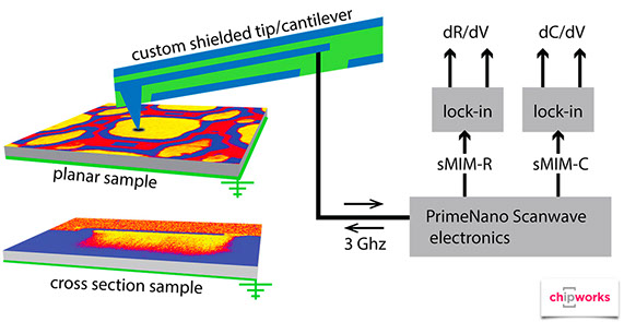
Figure 1 sMIM Hardware Simplified Schematic Diagram
The Chipworks’ ISTFA paper was co-authored with PrimeNano [1]. In this paper we compare and contrast the dC/dV-phase, dC/dV-amplitude, and sMIM-C signals that can be obtained simultaneously with the sMIM hardware. The paper includes cross-sectional and plan-view images of the pixels of the OmniVision OV2D7AG, which is a 175 kilo-pixel, global shutter, infrared CMOS image sensor (CIS) from the Amazon Fire Phone. The OV2D7AG is a front-side illuminated CIS. Localized CV curves were also measured. Both the OmniVision OV2D7AG and the Amazon Fire Phone have been analyzed in detail by Chipworks [2] [3] [4].
Figure 2 presents plan-view and cross-sectional SEM views of the OV2D7AG pixel. The cross section runs diagonally across the pixel array and includes the pixel transfer gate transistor.
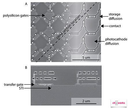
Figure 2 OmniVision OV2D7AG Plan-View and Cross-Sectional SEM of Pixel
The results of the sMIM scanning on the surface of the OV2D7AG, polished with a very shallow bevel to expose the near surface region, are shown in Figure 3. These three signals were acquired simultaneously. The regular array of pixels is clearly seen in these three images. The dC/dV signals are obtained by applying an AC bias to the tip-sample interface and then using a lock-in amplifier to detect the dC/dV signal. The dC/dV-phase signal (A) provides information on the carrier type beneath the scanning probe of the microscope, with P-type materials giving a positive signal (blue-purple) and N-type materials giving a negative signal (yellow). Highly doped and undoped materials give a null response (orange). The dC/dV-amplitude signal (B) is related to the carrier concentration; however, the amplitude signal is not monotonically related to the dopant level. As mentioned, the sMIM-C signal (C) varies monotonically with the carrier concentration, with non-conductive materials giving a small signal and highly doped materials giving a large signal.
The results of the sMIM scanning on the surface of the OV2D7AG, polished with a very shallow bevel to expose the near surface region, are shown in Figure 3.

Figure 3 Plan-View sMIM Images of CMOS Image Sensor Sample
Figure 4 presents cross-sectional sMIM images of the OV2D7AG pixel structure. The N-type photocathode of the pixels is clearly shown as the yellow feature in the dC/dV-phase images (A). A thin P-pinning layer lies between the photocathode and the overlying dielectric material. The photocathode and P-pinning structures can also be seen in the dC/dV-amplitude (B) and sMIM-C (C) images.
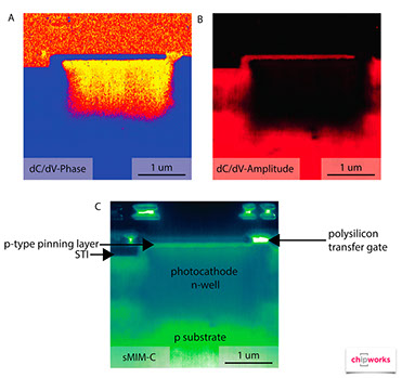
Figure 4 Cross-Sectional sMIM Images of CMOS Image Sensor Sample
These results are discussed in greater detail in our ISTFA 2015 paper, which is readily available from ASM International or on request from Chipworks [1].
sMIM is an exciting new technology which will bring great value to Chipworks’ clients. It is one of the only available techniques that can provide information on the dopant structures, and particularly the position of junctions, with deep sub-micron spatial resolution. The technique extends the capabilities of traditional SCM, due to the addition of several other imaging channels, including sMIM-C, which provides information on the dopant concentration, complementing the dopant type provided by the dC/dV-phase signal. A significant benefit of sMIM is the elimination of non-linear artifacts that often appear at PN junctions in conventional SCM images.
sMIM will bring value to both Chipworks’ competitive technical intelligence and our intellectual property clients, and in particular, to our image sensor clients. Supporting patents that involved doped structures has always been challenging since conventional dopant profile methods, such as spreading resistance profiling (SRP) and secondary ion mass spectrometry (SIMS), do not have sufficient spatial resolution, while conventional SCM was not able to provide information about the dopant levels involved. The sMIM technique will expand the range of patents that are supportable by reverse engineering since it provides better spatial resolution than conventional SCM, while also providing some information on the dopant levels.
References
- Benedict Drevniok, St. John Dixon-Warren, Oskar Amster, Stuart L Friedman, Yongliang Yang, Extending Electrical Scanning Probe Microscopy Measurements of Semiconductor Devices Using Microwave Impedance Microscopy, ISTFA 2015: Conference Proceedings from the 41st International Symposium for Testing and Failure Analysis, November 1–5, 2015, Portland, Oregon, USA, p, 77 (2015)
- OmniVision OV2D7AG 175 KP Global Shutter Infrared CMOS Image Sensor from the Amazon Fire Phone SCM Dopant Analysis, CWR-1410-902, Chipworks, 2014
- OmniVision OV2D7AG Global Shutter IR CIS (Dynamic Perspective Imager from Amazon Fire Phone) Device Essentials Image Set and Summary, DEF-1409-801, Chipworks, 2014
- Amazon SD4930UR Fire Phone Smartphone Basic Product Teardown Report, BPT-1408-801, Chipworks, 2014
A sample list of Benedict Drevniok’s recent publications:
- C Crudden & et al. “Simple Direct Formation of Self-assembled N-heterocyclic Carbene Monolayers on Gold and Their Application in Biosensing“. Nature Communications 7,12654 (2016) doi:10.1038/ncomms12654.
- DP Andrade & et al. “Surface and near surface defects in δ-doped Si (1 1 1)“. Journal of Physics: Condensed Matter 27, 125001 (2015).
- B Drevniok & et al. “Extending Electrical Scanning Probe Microscopy Measurements of Semiconductor Devices Using Microwave Impedance Microscopy“. ISTFA 2015: Proceedings from the 41st International Symposium for Testing and Failure Analysis, p. 77 (2015).
- C Crudden & et al. “Ultra stable self-assembled monolayers of N-heterocyclic carbenes on gold“. Nature Chemistry 6, 409–414 (2014) doi:10.1038/nchem.1891.
A sample list of St. J Warren-Dixon’s recent publications:
- SJ Dixon-Warren and B. Drevniok. “Practical Quantitative Scanning Microwave Impedance Microscopy”, ISTFA 2016 (in press).
- B Drevniok & et al. “Extending Electrical Scanning Probe Microscopy Measurements of Semiconductor Devices Using Microwave Impedance Microscopy“. ISTFA 2015: Proceedings from the 41st International Symposium for Testing and Failure Analysis, p. 77 (2015).
- R Alvis & el al. “Plasma FIB DualBeam™ Delayering for Atomic Force NanoProbing™ of 14nm FinFET Devices in an SRAM Array“. STFA 2015, p. 393.
- R Dhar & et al. “Direct Charge Measurements to Read Back Stored Data in Nonvolatile Memory Devices Using Scanning Capacitance Microscopy“. Journal of Vacuum Science & Technology B 31 , 061801 (2013).
Contact the authors: Benedict Drevniok – Chipworks, Oskar Amster – Prime Nano Inc., and St. J. Dixon-Warren – Chipworks

Copyright 2024. All Rights Reserved