Highest Resolution Electrical Measurements

Two Phases In In2Se3 Nano-ribbon
An In2Se3 nano ribbon is prepared with four metal contacts to determine the resistance across each of the ribbon segments. Figure 1 (a) is an SEM image of the nano ribbon. The image identifies the InAu leads and the In2Se3 nano ribbon. The nano ribbon appears uniform across its entire length. In the AFM topography image, (b), the In2Se3 ribbon also appears uniform along its length.
Electrical resistance measurements across the four contacts reveal that there is a large resistance, several orders of magnitude, from the lower segment to the topmost segment. The expected resistance between leads is uniform. The ScanWave™ sMIM-R image in (c) shows a contrast variation along the ribbon. The “light” and “dark” regions show that there are areas that have low resistance and high resistance respectively. The different contrast regions are associated with two known different phases of the In2Se3 material. These two phase are known to have different resistance values, one low and the other 2 orders of magnitude higher.
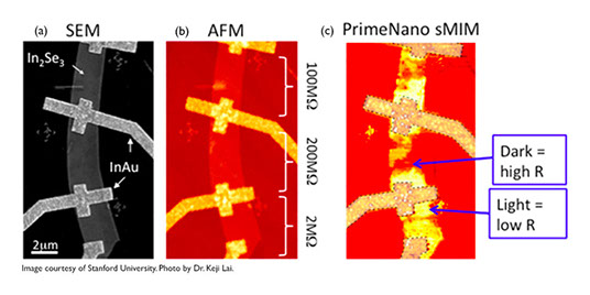
Figure 1. (a) an SEM image of the In2Se3 nano ribbon identifying the InAu contact pads and ribbon, (b) is an AFM topography image of the same In2Se3 nano ribbon. Direct measurements across the electrical contact leads with an external meter show orders of magnitude variation resistance from one segment of the nano ribbon to the other. Image (c) shows clear contrast of “light” and “dark” regions in the In2Se3 nano ribbon where phases of low resistance and high resistance material are revealed.
The In2Se3 material was also tested using a SIMS analysis technique. These subsequent measurements validated the presence of the two material phases of the In2Se3 nano ribbon. sMIM required no special sample preparation and was measured in ambient conditions. Similar results acquired in subsequent analysis required vacuum techniques and more intricate sample preparation. MIM presents a more direct workflow and quicker time to results.
Copyright 2024. All Rights Reserved