2K LT SCANWAVE™ - LOW TEMPERATURE sMIM SYSTEM
PrimeNano’s 2K LT ScanWave™ is a turnkey, industry robust solution for frontier physics research (quantum effects, phase transitions, etc.) and novel material studies (topological insulators, ferroelectrics, manganites, etc.). This system enables electrical characterization of materials at ultra-low temperatures and high magnetic field. This complete system solution reduces the researchers time to have the right equipment to get to their core research.
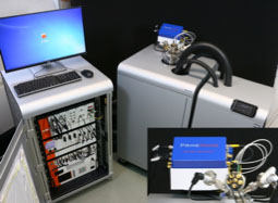
A complete integrated system, PrimeNano’s 2K LT ScanWave™
embedded key![]() components from cryogenic and high magnetic field SPM industry leader Attocube systems.
components from cryogenic and high magnetic field SPM industry leader Attocube systems.

Figure 1 2K LT ScanWave
Low Temperature / High Magnetic Field sMIM
A great deal of cutting edge physical investigations concerning fundamental mechanisms will frequently involve electrical measurements at low temperatures and high magnetic fields: the measurement of conductivity of novel material systems at varying temperatures was at the core of many Nobel Prize winning discoveries over the last thirty years, ranging from high temperature superconductivity (1987), quantum Hall (1985), fractional quantum Hall (1998), giant magnetoresistance (2007), and graphene (2010). More recently, being able to image electrical properties at the nano- and meso-scale has emerged as a fertile ground for discoveries. PrimeNano is the sole technology source for the successful and proven room temperature ScanWave™ module in a wide variety of applications at universities, national labs and industry [1-6].
Low-Temp sMIM System by PrimeNano
PrimeNano’s 2K LT ScanWave™ system utilizes key components from Attocube systems, a leader in the cryogenic and high magnetic field SPM. Key components were jointly developed and adapted for our application, while maintaining maximum compatibility. This turnkey ScanWave™ sMIM and SPM system allows researchers to focus on the research aspects without having to worry about the engineering aspects of such a complex system.
The standard system comes equipped with the 2K Low Temperature ScanWave™ sMIM electronics modules, optical interferometer feedback SPM insert, closed cycle cryostat, and superconducting magnet with computer-controlled interface. The system can be configured to have a closed loop SPM scanner, programmable closed-loop cryostat, multi-axis magnet up to 15T with liquid cryo option), and ultra-low temperature (using liquid He cryostat).


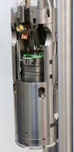
Figure 2
Left: cryostat insert with sMIM front end electronics and sMIM AFM head.
Right: Low Temp sMIM AFM with scanners, positioners and sMIM holder, sMIM matching network.
This first commercially available 2K LT ScanWave™ system implements sMIM at high field (e.g. 9 T) and variable temperature (down to ~2K). It creates an innovative experimental capability, enabling tremendous advancement in cutting edge physics research, as demonstrated by early sMIM work done at Stanford by the Shen group.
Such advances include: giant magnetoresistance characterization [7], quantum Hall effect in a 2D electron gas [8], quantum spin Hall effect [9], charge order [10], novel magnetic domain walls [11], and quantum Hall in graphene [12].
The 2K LT ScanWave™ tool provided by PrimeNano is shown in figure 2. This enables an unprecedented opportunity towards investigating and understanding the fundamental mechanisms associated with these phenomena at the nanoscale. 2K LT ScanWave™ is protected by 5 issued patents and more than 10 years of iterative product development.
The 2K LT ScanWave™ System dramatically lowers the barrier of entry to fundamental electrical measurements and will catalyze scientific discovery and advancement of materials-based technology. Up until recently the 2K LT ScanWave™ System only existed in 2 laboratories, which are collaborating groups of PrimeNano, that have contributed to the development. The Shen group has several publications in Science, PRL, and Nature Communications from one of the prototype cryogenic sMIM systems. These measurements can now be adopted by a multitude of physicists, physical chemists, materials scientists, etc., spanning academia as well as industry in both R&D and QA/QC applications.
Key Features
- Measure sub-micron variations in permittivity and conductivity and at ultra-low temp (down to 2K) and high B-Field (up to 15T)
- High stability temperature and magnetic field
- Versatile operation modes including sMIM, sMIM dC/dV, sMIM C-V spectrum for electrical properties characterization
Benefits
- Commercial turnkey solution for ultra-low temp high magnetic field sMIM and SPM
- Microscopy experiments in a cryogen-free, low vibration environment
- Fast exchange of samples and/or scanning probe tips
- Compatible with different AFM modes: contact, non-contact, constant height, constant force
- Minimize sample preparation
Example Use Cases
Solid state physics and quantum effects
- Phase transitions
- Topological insulators
- Quantum Hall effect
- Quantum spin Hall effect
Material science researches
- Ferroelectrics
- Manganites
1D/2D materials
- Domain walls
- Graphene
See Use Cases
See Use Cases
Technical Specifications
General Specification
Technology
Cryostat
AFM
Electrical measurement
Scanning Microwave Impedance Microscopy (sMIM)
Ultra-low vibration, pulse-tube based closed-cycle cryostat designed for scanning probe microscopy applications
Cantilever based AFM with interferometric deflection detection
sMIM near field measurement with DC/AC bias
Cryostat Specifications*
Temperature range
Superconducting magnet
Sample environment
Sample exchange
Usability
2..300K or 4..300K (depending on cryostat model)
9T (up to 12T optional)
Helium exchange gas
Top loading system for quick access
Fully automated temperature and magnetic field control via integrated touchscreen, USB interface for remote control
AFM Specifications**
Imaging modes
z feedback
Sample positioning travel range
Scan size
Measured RMS z-noise (constant force @ 4 K, 5 ms pixel time)
Insert Titanium housing diameter
Contact mode, non-contact mode, constant height, constant force
PI feedback loop for amplitude modulation (AM), phase modulation (PM) or frequency modulation (FM) using included PLL
5 x 5 x 5 mm3 (coarse positioning stage)
50 x 50 x 24 μm3 @ 300 K, 30 x 30 x 15 μm3 @ 4 K
< 0.10 nm (expected), < 0.15 nm (guaranteed)
48mm
sMIM Specifications
Measured parameters
Operation temperature
RF Operation frequency
Probe diameter
Spatial resolution
Electrical resolution
Microwave power to the tip
Bias
Probe
Compatible modes
S11, sMIM (C, R) sMIM-AC (dC/dV, dR/dV) Amp & Phase
1.5..300K or 4..300K (depending on cryostat model)
3GHz (nominal)
<100nm
100nm (depends on sample)
1aF
-15dBm to -45dBm
+/-5V, DC-150kHz
Proprietary coax shielded probe
MFM, KPFM, PFM, & c-AFM
* Integration in cooperation with Attocube. Cryostat specifications based on partner verified performance
** AFM specifications based on modified Attocube SPM insert from Attocube
References
- M. Tuteja, P. Koirala, S. MacLaren, R. Collins, A. Rockett. Direct observation of electrical properties of grain boundaries in sputter-deposited CdTe using scan-probe microwave reflectivity based capacitance measurements. App. Phys. Lett, 107, 142196 (2015)
- A. Tselve, A. Klein, J. Gassmann, S. Jesse, Q. Li, S. Kalinin, N. Balke. Quantitative Nanometer-Scale Mapping of Dielectric Tunability. Advanced Materials Interfaces, 1500088 (2015)
- T. Monti, A. Tselev, O. Udooudo, I.N. Ivanov, S.W. Kingman. High-resolution dielectric characterization of minerals: a step towards understanding the basic interactions between microwaves and rocks. http://arxiv.org/abs/1510.08619
- W.L. Wilson, E. Seabron, S. Maclaren, X. Xie, S.V. Rotkin, J. A. Rogers. Scan-Probe Microwave Reflectance of Horizontally Aligned Arrays of Single-Walled Carbon Nanotubes: Nanoscale Imaging of SWNT Electrical Properties in the Quantum Regime. ECS conference (2015). MA2015-01 769. http://ma.ecsdl.org/content/MA2015-01/6/769.abstract
- B. Drevniok, S. Dixon-Warren, O. Amster, S.L. Friedman, Y. Yang. Extending Electrical Scanning Probe Microscopy Measurements of Semiconductor Devices using Microwave Impedance Microscopy. ISTFA 2015. In press.
- S.L. Friedman, O. Amster, Y. Yang. Recent advances in scanning Microwave Impedance Microscopy (sMIM) for nano-scale measurements and industrial applications. Proc. SPIE 9173, Instrumentation, Metrology, and Standards for Nanomanufacturing, Optics, and Semiconductors VIII, 917308 (August 27, 2014)
- K.J. Lai, M. Nakamura, W. Kundhihanjana, M. Kawasaki, Y. Tokura, M.A. Kelly, Z.X. Shen. Mesoscopic Percolation Resistance Network in a Strained Manganite Thin Film. Science, 329, 190 (2010).
- K.J. Lai, W. Kundhijanjana, M.A. Kelly, Z.X. Shen, J. Shabani, and M. Shayegan. Imaging of Coulomb Driven Quantum Hall Edge Stripes. Physical Review Letters, 107, 176809 (2011)
- E.Y. Ma, M.R. Calvo, J. Wang, B. Lian, M.Muhlbauer, C. Brune, Y.T. Cui, K. Lai, W. Kundhikanjana, YL Yang, M. Baenninger, M. Konig, C. Ames, H. Buhmann, P. Leubner, L.W. Molenkamp, S.C. Zhang, D. Goldhaber-Gordon, M.A. Kelly, Z.X. Shen. Unexpected edge conduction in mercury telluride quantum wells under broken time-reversal symmetry. Nature Communications, 6, 7252 (2015).
- E.Y. Ma, B. Bryant, Y. Tokunaga, G. Aeppli, Y. Tokura, Z.X. Shen. Charge-order domain walls with enhanced conductivity in a layered manganite. Nature Communications, V6, 7595 (July 2015)
- E.Y. Ma, Y.T. Cui, K. Ueda, S.J. Tang, K. Chen, N. Tamura, PM Wu, J. Fujioka, Y. Tolura, Z.X. Shen. Mobile metallic domain walls in an all-in-all-out magnetic insulator. Science, 350, 538-541 (2015)
- Y.T. Cui, B. Wen, E.Y. May, G. Diankov, Z. Han, F. Amet, T. Taniguchi, K. Watanbe, D. Goldhaber-Gordon, C.R. Dean, Z.X. Shen. Unconventional Correlation between Quantum Hall Transport Quantization and Bulk State Filling in Gated Graphene Devices. http://arxiv.org/abs/1511.01541
Copyright 2024. All Rights Reserved
