Characterization Of Compound Semiconductor SiC
Alternative semiconducting materials are increasingly important for a range of consumer devices and industrial applications. Ge, GaAs, SiC, GaN and InP are some of the more common compound semiconductor materials. These alternative semiconductor materials are used in a range of applications ranging from faster switching of signals than can be achieved by Si designs; applications requiring high current densities or power such as used in communications technology, energy, lighting, transportation and industrial manufacturing.
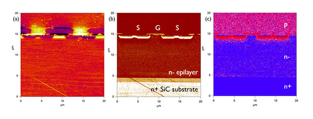
Below is an example of a SiC transitor cross-sectioned and polished to expose the active doped regions. Figure 1 shows the (a) topography, (b) the dC/dV Amplitude representing the carrier concentration, (c) the dC/dV phase, which gives the carrier type (n- or p-type). The scanned area is 20μm x 20μm. The Amplitude image shows the gate and source regions with the transition to the substrate n- doped region. At the bottom of the image there are two more transitions including the drain plain. The phase image shows the two carrier polarities, p-type as red and n-type as blue.

Figure 1. Example of a cross-section SiC sample imaged using the ScanWave™ sMIM module on an Oxford Instruments Asylum Research Cypher AFM. Figure (a) is the topography, (b) is the dC/dV amplitude doping concentration; (c) is the dC/dV Phase differentiating the n and p doped regions.
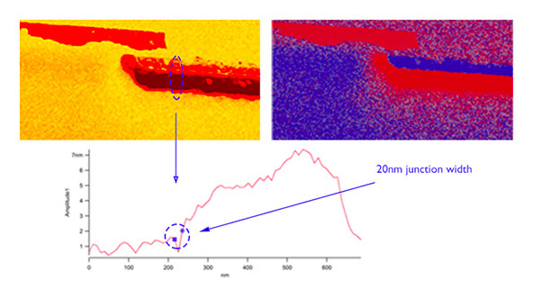
Figure 2 is a higher resolution image of the same SiC transistor device shown above. The scanned area is 5μm x 2.5μm. Image (a) shows the dC/dV Amplitude doping concentration and (b) shows the dC/dV Phase carrier polarity. The contrast in the dC/dV Amplitude image shows a fine line at the junction transition form the n-source to p-well and then to the substrate n-. A line profile is taken across the p-n junction in Figure 2 (c); the line profile shows the gap, junction length, of the n-p source junction. The gap measures < 20nm. In the phase image (b), a the clear “good” phase signal differentiates the two carrier types. The p-carrier is shown in the gate anode region and p-well of the source; the n-carrier type is shown in the n-Source and the n- epilayer. In the bottom portion of the image there is a stronger phase signal that represents the n+ SiC substrate region.

Figure 2. shows the same SiC transistor in a higher resolution image, 5μm x 2.5μm. The left image, (a), is the sMIM dC/dV Amplitude representing the carrier concentration. The right image, (b), presents the dC/dV phase representing the carrier type. The phase data shows the carrier types in the gate region. (c) A measurement of the gate junction is approximately 20nm.
Copyright 2024. All Rights Reserved
