Characterization Of Front Side Polish SRAM
A commercially available SRAM reference sample developed by C. Nakakura’s group at the Sandia National Lab, was developed as a reference to help baseline the operation of SCM measurements. This sample has become a widely used reference to confirm basic capabilities to image a doped sample and differentiate the carrier types and various doping levels on the device.
The MIM mode has an analogous capability to SCM, dC/dV through which two additional channels of data, the Amplitude and Phase, corresponding to the carrier concentration and carrier type respectively are collected. Below is presented an example of sMIM measurements on the SRAM sample.
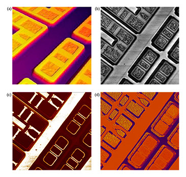
Figure 1 (a) below shows the topography in 3D rendering. The area imaged is 20×20 μm using contact mode. The three images along the bottom show, from left to right, the sMIM –C (capacitive) image; the amplitude dC/dV image – carrier concentration distribution; and phase of dC/dV image – the carrier polarity or charge respectively.

Figure 1 Images of a standard reference sample used for SCM to determine baseline capabilities for doping concentration and carrier type. This well understood and commercially available sample is used to also baseline the sMIM dC/dV amplitude and Phase. (a) 3D rendering of the topography; (b) sMIM-C image; (c) is the dC/dV Amplitude representing the carrier concentration; and (d) is the dC/dV Phase image representing the carrier type, n-doped is blue and p-doped is red.
These images show very good SNR of the doped regions and differentiate the n & p regions as expected.
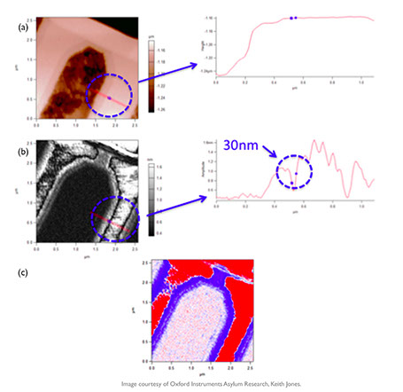
Figure 2 is a higher resolution image of the SRAM highlighting a known junction of the “O” memory feature. The area images is 2.5 x 2.5μm. The line profile is taken across the p-n junction. The line profile does not show any specific features. In the image below, the dC/dV Amplitude, the p-n junction is clearly defined. A line profile across the junction measure approximately 30nm. The image (c) shows the dC/dV Phase. This image gives the carrier type. We expect to see strong signals in the n-doped and p-doped regions. The red color is p-doped and blue represents the n-doped carriers.

Figure 2 High resolution image of the SRAm across a known gate junction. Image (a) is the topography with a line profile accros the gate feature. No physical feature is seen in the profile. In (b) the dC/dV Amplitude image the junction is very well defined. The line profile is take across the same location as in (a). The junction is measured approximately 30nm across. Image (c) is the dC/dV Phase. The image shows the carrier type, the red represent the p-type and the blue the n-type dopong.
Copyright 2024. All Rights Reserved
