Conductivity Studies Of Graphene
Graphene has attracted enormous interest and intense research activities due to its rich physical properties in fundamental research and versatile potentiality to revolutionize many applications, especially in electronics and opto-electronics1,2,3. The unique properties of graphene for electrical applications makes it a focal point for next generation microelectronics. Imaging the electrical properties of graphene presents specific challenges to researchers. sMIM reduces the technical difficulties of preparing often small flakes or films on non-conducting substrates for electrical measurement by eliminating the need for a conductive path. sMIM directly probes the grain structures and local variations in conductivity differentiating between conductive, semi conductive, and insulating regions. Below are presented several examples of sMIM measurements on differently prepared graphene.
Moire Patterns on Single Layer Graphene deposited on BN
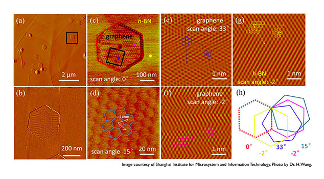
Precisely aligned graphene on h-BN without a metal catalyst was found under very specific crystal orientations of the graphene layer to the h-BN layer to result in Moire interference patterns1. Results shown in the work by Tang, Wang, and Zhang et al imaging with lateral force microscopy visualized these Moire patterns confirming the specific conditions and tying this to the stress relief of the graphene Van der Waals force between the two epitaxy layers. In follow-up research done at Stanford University and PrimeNano in cooperation with SIMIT’s Dr. Wang and Dr. Tang the Moire patterns were reproduced using sMIM.

Figure 1 are the results from the journal article reference 1 presenting the AFM topography and lateral Force images of the graphene flake, Moire pattern, and atomic lattice orientation respectively.
The following is the Figure 1 description from Tang et al article. “Determination of the rotational orientation of monolayer graphene with respect to h-BN. (a) A typical topography of the graphene grains on h-BN surface. Almost all the grains are in hexagonal shape with the opposite sides parallel. The hexagons are aligned on the whole h-BN surface. It clearly indicates anisotropic growth of graphene; (b) A zoom-in view from the black box in panel (a). A sizable superstructure with a periodicity much larger than the lattice constant of both graphene and h-BN was observed on graphene; (c) Friction image of a single crystal graphene on h-BN. Dashed red line marks the edges of this grain; (d) A closer view (100 3 100 nm2) in the black box of (c), the superstructure exhibits hexagonal symmetry with lattice constant about 14 nm; Regular hexagons are superimposed on the images to demonstrate the giant lattice. The friction images (e), (f) and (g) show the atomic lattice of 535 nm2 area taken from the blue, pink and orange dot areas in panel(c), regular hexagons demonstrate the lattice of both graphene and h-BN, respectively. Zigzag directions (in dashed line) and lattice vectors (in solid line) are indicated by arrows.”

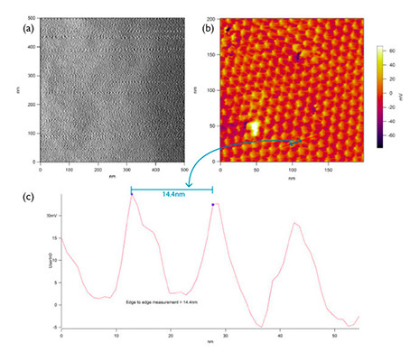
Figure 2 (a) Topography image 500nm x 500nm area in region of Moire pattern. No Moire pattern is visible with the topographic imaging. (b) MIM image 200nm x 200nm area using contact mode for imaging. The hexagonal structures are clearly evident. (c) Line profile taken from MIM image along 3 hexagon Moire features. Edge to edge measurement shows 14.4 nm features and high quality SNR for the electrical measurement. The MIM demonstrates sub 10nm resolution for these highly conductive samples
Figure 2 (a) shows an sMIM image of the same Moiré pattern formed by the lattice mismatch of the graphene monolayer and the h-BN film. sMIM proved to be a an easier and much more repeatable method of visualizing the Moire pattern than with lateral force (LFM) or topography imaging. The line profile shown below in Figure 2 (c) is taken across several of the hexagonal Moire structures. The cross-section measured 14.4nm, matching the LFM measured distance and the calculated values from the previous work. The individual hexagonal features demonstrate that on these very flat highly conductive samples approximately 5nm resolution is achieved.
Analysis of the hexagon Moire structures with sMIM shows brighter (more conductive) at the edges of the hexagon. Further work by Tang and Wang of SIMIT focus correlating the conductivity of the graphene to the stress induced by the lattice mismatch between the graphene and h-BN.
Conclusion
sMIM is shown to be a versatile technique for researchers to probe the electrical properties of graphene. Graphene has proved a challenging material to prepare and study especially for electrical properties where conventional methods require a conductive path or ground. The microwave frequency regime removes the need for a sample to be grounded or provide a conductive path to the instrument. MIM measurements are able to image variations in the sample conductivity over a very large range, a particular property of graphed research, where one region can have very low conductivity and another be orders of magnitude higher. An example, measurements on a single layer graphene deposited on BN, using PrimeNano’s ScanWave™ system has been presented in order to demonstrate the versatility and sensitivity of the MIM technology.
References
- S. Tang, H. Wang et al, Precisely aligned graphene grown on hexagonal boron nitride by catalyst free chemical vapor deposition, Scientific Reports. 3: 2666 (2013)
- Geim, A. K. & Novoselov, K. S. The rise of graphene. Nature Mater. 6, 183–191 (2007).)
- Novoselov, K. S. et al. A roadmap for graphene. Nature 490, 192–200 (2012).)
Want to read more? Download the complete paper of this study.
Copyright 2024. All Rights Reserved
