Microwave AC Conductivity Of Domain Walls In Ferroelectric Thin Films

Dr. Alexander Tselev received his PhD in Materials Sciences from Dresden University of Technology, Germany. He spent terms at University of Maryland, College Park, Georgetown University, Duke University, and the Center for Nanophase Materials Sciences at ORNL in University of Tennessee, Knoxville. Currently his primary research focus is on near-field microwave microscopy and complex oxide thin films. He has published more than 150 papers in refereed journals.
In this just appeared paper in Nature Communications co-led by Dr. Alexander Tselev and Dr. Petro Maksymovych from ORNL’s Center for Nanophase Materials Sciences, it is shown that employing high-frequency ac conduction can open up new technological opportunities for oxide electronics as well as in harnessing electronic properties of materials with a poor dc conduction, especially at the nanoscale.
Microwave AC Conductivity of Domain Walls in Ferroelectric Thin Films
By Alexander Tselev et al. Nature Communications, 2016

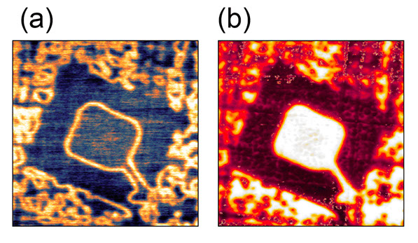
(a) sMIM conduction image of the box-in-box domain structure written by the sMIM probe on a Pb(Zr0.2Ti0.8)O3 (100) film. Spontaneous domains and domain walls seen around the structure were erased inside the structure during writing; the domain walls of the structure as well as the spontaneous domain walls are conducting. (b) Combined out-of-plane piezoresponse force microscopy image acquired right after the image in (a). The image reveals ferroelectric domains with up and down directions of ferroelectric polarization. Image size is 6 μm × 6 μm.
In ferroelectrics, domains of uniform polarization and domain walls separating them can be created and reconfigured by electric fields. The thickness of the domain walls is only a few nm. Combination of these two properties makes ferroelectric domain walls attractive candidates for building blocks in future logic and memory electronic devices. Recently, a number of high-profile reports claimed the existence of mobile charge carriers at ferroelectric domain walls. However, so far, in nanoscale measurements at dc, ferroelectric domain walls were seen as highly insulating – preventing their nondestructive readout and possible applications as well as hiding the physical reasons of the domain wall conductivity. The study published in Nature Communications revealed that domain walls in thin films of two different ferroelectrics, lead zirconate titanate and bismuth ferrite, exhibit large conductance at microwave frequencies. The conductivity was found in nominally uncharged domain walls in these conventional ferroelectrics, which is unexpected within today’s models of conducting domain walls. An estimate of the wall ac conductivity at 3 GHz yields that it is much higher than previously inferred and enhanced by ~100 times at microwave frequencies compared to direct current. The authors, therefore, detected a new conduction regime that may be incompatible with direct current. The approach for the first time enabled a completely non-destructive electronic read-out of domain walls in ferroelectrics that does not perturb their structure over hours and days. To explain their findings, the authors note that generally conductivity at gigahertz frequencies can be larger by orders of magnitude than at dc. A fundamental reason behind this enhancement is that charge carriers localized by energy barriers at dc can contribute to ac conduction by oscillating between the barriers at high frequencies. A domain wall roughening by crystal lattice defects in the films was invoked to explain the high ac conduction of domain walls. Furthermore, it is argued that the ac conduction is immune to large contact resistance, which enables sensitive detection of a domain wall without changes to its local structure.
Although the paper is focused on ferroelectric domain walls, its conclusions are much broader. These findings reveal that new opportunities and device paradigms for oxide electronics can be envisioned in the microwave domain as well as new insights into outstanding scientific questions in complex and nanoscale electronic materials. The work demonstrates a strong and presently unrealized potential of high-frequency conduction for basic nanoscale physics, materials science, and a great number of future applications.
To read the original publication of this paper, please visit Nature Communications.
Dr. Alexander Tselev’s Research
The groundbreaking research and recent publications of Dr. Tselev demonstrates the exciting new categories of research were Scanning Microwave Impedance Microscopy (sMIM) opens new ground to the research community, both for advanced materials research and commercial applications. PrimeNano applauses Dr. Tselev’s novel application of sMIM technology and look forward to where his creativity will lead the field in the future.
A sample list of Dr. Tselev’s recent publications:
- T Monti & et al. “High-resolution dielectric characterization of minerals: a step towards understanding the basic interactions between microwaves and rocks”. International Journal of Mineral Processing 151, 8–21 (2016); http://dx.doi.org/10.1016/j.minpro.2016.04.003.
- A Tselev & et al. “Seeing through walls at the nanoscale: Microwave microscopy of enclosed objects and processes in liquids”. ACS Nano 10, 3562–3570 (2016); DOI: http://dx.doi.org/10.1021/acsnano.5b07919.
- A Tselev & et al. “Surface control of epitaxial manganite films via oxygen pressure”. ACS Nano 9 (4), 4316-4327 (2015); http://dx.doi.org/10.1021/acsnano.5b00743.
- A Tselev & et al. “Quantitative nanometer-scale mapping of dielectric tunability”. Advanced Materials Interfaces 2, 1500088 (2015); http://dx.doi.org/10.1002/admi.201500088.
- L Collins & et al. “Probing charge screening dynamics and electrochemical processes at the solid-liquid interface with electrochemical force microscopy”. Nature Communications 5 (2014); http://dx.doi.org/10.1038/ncomms4871.
- A Tselev & et al. “Scanning Near-field microwave microscopy of VO2 and chemical vapor deposition graphene”. Advanced Functional Materials 23 (20), 2635-2645 (2013); http://dx.doi.org/10.1002/adfm.201203435.
Contact the author: Dr. Alexander Tselev.
Copyright 2024. All Rights Reserved
