Doped Semiconductors

Cross-section View of a 1.1μm Pixel CMOS Image Sensor

This is a cross-section view of a 1.1um pixel Samsun CMOS image sensor. The image is a high contrast sMIM-C Image That clearly differentiates the n-and p-type carrier regions and individual pixel transitions. Of particular interest is the uniformity of the doping region in the blue photo cathode region. Image courtesy of Chipworks Corporate.

14nm node logic FinFET

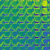
sMIM dC/dV Amplitude of a 14nm node logic FinFET. Image courtesy of Chipworks Corporate.

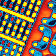
Front-side Illuminated Global-shutter CMOS Sensor from a Common Cell Phone

Planar view of a 2.5um pixel CMOS image sensor deprocessed to bare silicon. The sMIM-C image shows both the doped n-type and p-type regions as well as the highly doped STI and poly-gate regions. Image courtesy of Chipworks Corporate.

Cross-section a CMOS Image Sensor Pixel Structure

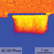
The cross-sectional sMIM-R image of a CNT’s OV2D7AG pixel structure using Bruker ICON AFM Peak Force Tapping mode. The N-type photocathode of the pixels is clearly shown as the yellow feature. A thin P-pinning layer lies between the photocathode and the overlying dielectric material. Image courtesy of Chipworks Corporate and PrimeNano Inc.

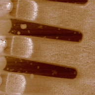
Cross-section Polished IGBT Power Device (Peak Force Tapping Mode)

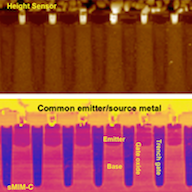
sMIM-C with corresponding height image of an IGBT power device cross-section polished imaged using Bruker ICON AFM Peak Force Tapping mode. Image courtesy of Bruker Nano Inc.

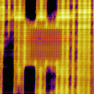
Stored Charge in a Backside Polished FPGA

sMIM image of a backside polished FPGA FLASH memory array. The red regions show where the FLASH cells have stored charge.

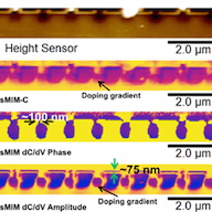
Cross-section CMOS Sensor

Image of a cross-section CMOS sensor using Bruker’s ICON AFM to image simultaneous Height image, sMIM-C and corresponding dC/dV amplitude and phase data highlighting the doping regions and relative concentration. Image courtesy of Bruker Nano Inc.

Backside Polished FPGA – Imaging Stored Charge on a Flash RAM Array

sMIM-R data revealing stored charge in a FLASH memory array imaged from the backside after polishing the Si to an approximate 100nm thickness. The data were acquired using an Oxford Instruments Asylum Research Cypher AFM in non-contact mode utilizing a 2nd internal lock-in amplifier synced to the same frequency as the mechanical resonance of the cantilever. The result is a dC/dZ image sensitive to the presence of strored charge in a single cell. The red color cells show where the charge is present.

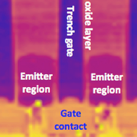
Insulated Gate Bipolar Transistor (IGBT)

Image is the sMIM dC/dV Amplitude signal of a vertical Insulated gate bipolar transitor (IGBT). The sampe was imaged using a 1V AC bias applied between tip and sample. The dC/dV amplitude is sensitive to the doping concentration of the cross-sectioned devices. The image shown has a very high level of detail for the emmiter, gate metals, and even at the high doped region of the gate region with oxide interface.

Buried Grating under 100nm Si from a Back-side Polished Logic Device

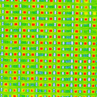
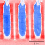
Image of sMIM-C channel showing a buried grating structure under 100nm of silicon wafer left after backside polishing the die of logic devices. The grating structure has a fine pitch of 250nm spacing. The sMIM-C image shows defects and other details that confirm a resolution less than 100nm, even though the image was acquired through the 100nm thickness of the Si over-layer.

Cross-section Polished IGBT Power Device (Imaged in PFT Mode)

sMIM-C image of an IGBT power device cross-section polished imaged using PFT mode. Image courtesy of Bruker Nano Inc.
Copyright 2024. All Rights Reserved