TECHNOLOGY

Conductivity

Variations in conductivity or resistivity

Permittivity

Variations in local dielectric properties

Dopant Concentration

Carrier concentration and carrier type

ScanWave™ Advantages

   Unprecedented Sensitivity

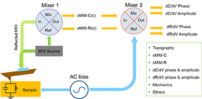
   Single scan – 7 channels of data

   Nano Resolution

Industry’s highest sensitivity lets you image the hard stuff. Industry’s lowest noise floor lets you see the small stuff.
  • Localized Relative
    • Permittivity ε & Conductivity σ
    • Dopant Concentration & Type
    • Direction & Magnitude of dR
  • Topography
Transform your AFM into a high resolution, nanoscale local electrical property microscope.
   Subsurface Imaging

   Measure different materials, simultaneously

   Minimal to no Sample Prep Required

Imaging of structures buried underneath the sample surface is possible thanks to the long range nature of ScanWave.

Be it conductors, semiconductors, dielectrics, or insulators, ScanWave™ can handle it all. Different materials, even of different classes, can be imaged in the same scan.

The sample can be imaged without a conductive path or current flow or even exposed. Therefore, little to no sample prep is needed.

   No Conductive Path Needed

   Contact and Non-Contact Mode Imaging

   Easy to Use Software

No ground or conductive path needed to get your electrical characterization.
Electrical measurements can be made in most AFM modes such as Contact, Non-Contact, Tapping, PeakForce Tapping, Lift Mode and Datacube.
Scan management and configuration is a bliss.

Scanning Microwave Impedance Microscopy (sMIM)

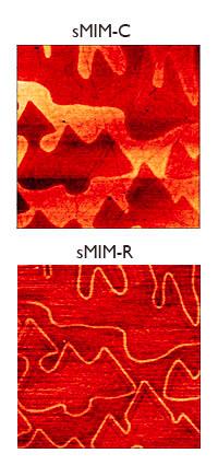
Scanning Microwave Impedance Microscopy (sMIM) is a new mode of imaging using an atomic force microscope (AFM). PrimeNano’s ScanWave sMIM modules produce high quality images of local electrical properties with better than 10 nm resolution. The core of our technical approach is to utilize microwave reflections from a nanometer scale region of the sample directly under the sMIM probe. The magnitude and phase of these reflections is dominated by the local electrical properties. The ScanWave sMIM measures these reflections as a function of position to create images of variations in dielectric constant and conductivity.


The ScanWave™ system provides multiple channels as output to the host AFM that can then be viewed as images in the AFM software. The sMIM signals represent the permittivity (ε) and the conductivity (σ) of the imaged area. If the sample is a doped semiconductor (a nonlinear) material, ScanWave™ can provide the carrier concentration and carrier type (n or p) as well as the direction and magnitude or dR.
Why Microwave Frequencies
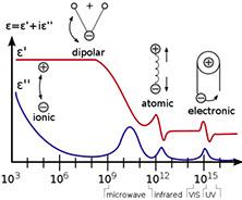
Using Microwave frequencies to look at a material’s dielectric constant and conductivity gives a high degree of contrast compared to other radiation energies. They are particularly good at probing the energetics of localized σ and ε without disturbing the sample’s intrinsic properties. Also due to their long wavelengths, microwaves have a useful long range sensitivity (> 200 nm) which can image buried structures. This allows the scanning of a sample in either a contact or non-contact mode. Additionally, sMIM does not require external electrical contact or grounding and can be used on insulating substrates.

How ScanWave™ Works

  1. ScanWave™ sends microwaves to the probe tip via a fully shielded path
  2. The microwaves create a near-field electromagnetic wave at the the probe tip that interacts with the sample surface and subsurface
  3. After the near-field interacts with the sample, a portion of the microwave power is reflected back through the same shielded path to the ScanWave™ electronics for filtering, demodulating, and processing
  4. As the probe moves across the sample, the reflected microwaves vary in amplitude and phase due to variations in the local electrical properties under the probe tip
  5. The ScanWave™ software calibratesthe reflected signal from the probe-sample interface to create a capacitive and a resistive image that are in turn displayed by the AFM simultaneously with the topography image(s).

Our Probes

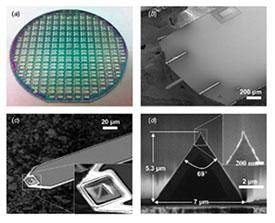
PrimeNano manufactures its own shielded probes. We use a wafer scale MEMS fabrication process to manufacture probes with co-axially shielded cantilevers and solid metal probe tips. The probes are coated with metal on both sides and have a center conductive line. The probes are supplied with a 25nm tip radius to balance the requirements of topographical resolution and sensitivity of the electrical signal. Since this is a near-field signal response, it is dependent on the volume of material in the localized electromagnetic field at the probe tip-sample interface. If the tip is too sharp the reflected signal is too small. The typical spatial resolution of the electrical measurements depends somewhat on the electrical properties of the sample. For example, for doped and metallic samples we have resolved electrical features below 10 nm. See our Application section for examples of actual sMIM measurements or visit our Probe Store.

Literature On ScanWave™

For a list of ScanWave™ or sMIM related research, please download our reference list.
Copyright 2024. All Rights Reserved