APPLICATIONS

Research Based On ScanWaveTM
For a list of ScanWave™ or sMIM related research, please download our reference list.

Low Dopant Level Measurements in Semiconductors

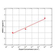
In this study, phosphorus was the species used which is an n-type dopant in silicon. Not only did we demonstrated the absolute sensitivity of sMIM’s permittivity and conductivity measurements in all concentration levels, but also its outstanding performance in low doped silicon (well below 1E15 a/cm3 levels). An additional advantage of sMIM is that there are no limitations due to species and matrix interactions so any type of dopant can be imaged at the same level of sensitivity.

Characterization of Insulated-Gate Bipolar Transistor (IGBT)

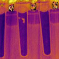
Investigation of the electrical parameters of an Insulated-Gate Bipolar Transistor (IGBT). sMIM images of IGBT devices reveal a high level of device detail across all material classes: metals, doped regions, and insulator materials. Simultaneous acquisition of the dC/dV signal provides dopant concentration variation and carrier type. ScanWave™ has higher measurement sensitivity than other electrical characterization methods typically used for investigation of semiconductor devices.

Characterization of Front Side Polish SRAM

SRAM sample used as a reference to confirm basic capability to image a doped sample and differentiate the carrier types and doping levels on the device. sMIM measurements show a Junction gap 30nm is well resolved.

Characterization of Compound Semiconductor SiC

Images of silicon carbide (SiC) devices using ScanWave™ integrated on an Asylum Research Cypher AFM. Results show differentiation carrier concentration and carrier type in the dC/dV Amplitude and Phase images respectively. The high-resolution results reveal junction gaps as small as 20nm.

Buried SiO2 Structures under Si3N4 Film

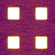
PrimeNano fabricated a test sample to illustrate sensitivity to local permittivity even when buried beneath the sample surface. The sample contains patterned SiO2 structures under a Si3N4 film. The nitride surface was polished to eliminate any residual topographic features.

Two Phases in In2Se3 Nano-ribbon

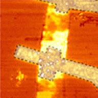
Determining the presence and distribution of resistivity variation in an In2Se3 nano-ribbon, explaining unexpected variations in transport measurements. sMIM images show 2 phases of the In2Se3 nano ribbon associated with two different conductivities. ScanWave™ provides electrical characterization of nano-ribbon material without special sample preparation and in ambient conditions.

Spontaneous Domain Walls in Ferroelectric crystals

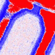
ScanWave™ supports simultaneous imaging of the nano-mechanical properties of the ceramic materials and the sMIM electrical properties, including features such as domain wall conductivity that are not detected with other electrical methods.

Conductivity Studies on Graphene

Examples of sMIM images on graphene identifying domains and regions of varying conductivity. sMIM reduces the technical difficulties of preparing often small flakes or films on non-conducting substrates for electrical measurement by eliminating the need for a conductive path to ground.

Buried Stored Charge in SRAM Flash Memory

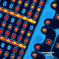
Sensitivity validation of sMIM on imaging stored charge in a backside polished FLASH RAM array. The FLASH array of commercially available FPGA device was programmed with a systematic pattern of 1’s and 0’s. The sample was then depackaged and polished from the backside with a shallow bevel. sMIM is shown to image the stored charge with high degree of contrast through a 100nm thick residual Si layer.
Copyright 2024. All Rights Reserved